Our new, safer-to-use-with-higher-currents, PCBs arrived from the fab house this week.
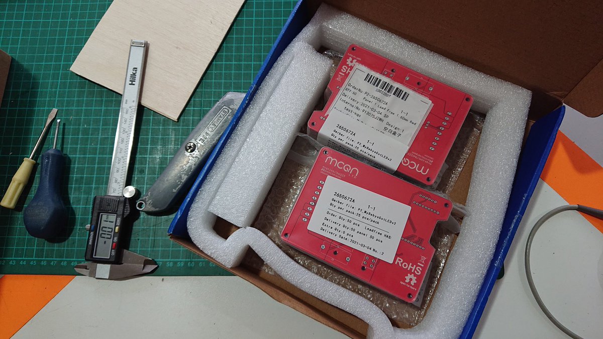
Given we haven't had anything to sell since discovering the problem, getting them soldered up and tested was top priority.
So we interrupted Arthur's work on the Totaliser prototype to teach him the ways of the reflow oven and how to solder up boards. That let us solder up a few test boards to double-check that I'd not made any stupid mistakes in the new layout.
Thankfully the new boards passed with flying colours, and Arthur returned to work on the Totaliser while I ran through soldering up a batch of boards ready to stick in our Tindie store. I recorded a little timelapse of the process:
There's a brief pause in the middle of that video where I'm running the first boards through the oven whilst also on a videocall. That was about some potential new work to update and expand on a project we did a few years back. It was good working with them previously, and this will be an interesting update, assuming it goes ahead.
Arthur didn't quite get the Totaliser finished, thanks to the interruptions, but has some super nice living hinge design for the case worked out and most of the case worked up in CAD and ready to cut.
And to wrap up these weeknotes, a mention of an interesting Twitter conversation we were involved in about the environmental impact of electronics and life-cycle assessments.
I don't know of any tools like that, but would love to hear of any, and would be up for helping build them too. It's something I'd like us to work out and share for @MCQN_Ltd's products (among a bunch of other info like security/privacy, etc.) https://t.co/D4e3NenS1c
— Adrian McEwen (@amcewen) March 9, 2021
There weren't any firm conclusions from it, but we got some useful pointers to resources and things to consider. It's something that we want to start producing as a standard part of our product development process, and then work to make it better. If anyone has experience with this or pointers, then please shout!